炭化珪素基板の加工は難しいが、単結晶炭化珪素の電子部品への応用が今後の発展の方向となり、炭化珪素デバイスの大規模応用・普及が進むよう、困難な炭化ケイ素加工の問題を解決する方法を見つける必要がある
。
現在、SiC材料加工技術には主に方向性切断、チップ粗研削、精密研削、機械研磨、化学機械研磨(精密研磨)のプロセスがあります。このうち、化学機械研磨は最終プロセスであり、そのプロセス方法の選択、プロセスルートの配置、およびプロセスパラメータの最適化は、研磨効率とプロセスコストに直接影響します。
ただし、SiC 材料は硬度が高く化学的安定性が高いため、従来の CMP 研磨プロセスでは材料の除去速度が低くなります。したがって、産業界は、以下に示すように、プラズマ支援、触媒支援、紫外線支援、および電場支援を含む、平坦化超精密加工技術をサポートする補助効率技術の研究を開始した。
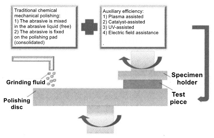
01 プラズマ支援技術
山村和毅 ほかこれは、プラズマによって表面材料を酸化してより柔らかい酸化物層にする補助的な化学機械研磨であり、同時に摩耗による摩擦や磨耗によって材料を除去するものである [21]。
基本原理は次のとおりです。RF 発生器の反応ガス (水蒸気、O など) を介して、自由基 (OH 遊離基、O フリーラジカルなど) を含むプラズマを生成し、表面上の遊離基の強力な酸化能力を高めます。 SiC材料の表面を酸化改質します。柔らかい酸化物層が得られ、その後、柔らかい研磨剤(CeO2、Al2O3など)で研磨することによって酸化物層が除去され、SiC材料の表面が原子レベルの滑らかな表面に達します。しかし、PAP プロセス試験装置の価格と処理コストが高いため、SiC チップを処理する PAP プロセスの促進も制限されています。[25]
02 触媒支援プロセス
産業分野では、SiC結晶材料の高効率超精密加工技術を研究するために、研究者は触媒支援化学機械研磨用試薬を使用しています。材料除去の基本メカニズムは、試薬の触媒作用により SiC 表面に柔らかい酸化物層が形成され、研磨剤の機械的除去によって酸化物層が除去されることです。高品位な表面を実現します。文献では、ダイヤモンド W0.5 を研磨剤として使用する化学機械研磨技術の強化を支援するために、Fe3O4 触媒と H2O2 酸化剤が使用されています。最適化後、研磨速度12.0mg/hで表面粗さRa=2.0〜2.5nmが得られた31)。
03 UV アシスト技術
SiC表面の平坦化加工技術を向上させるため。研究者の中には、化学機械研磨プロセスにおける触媒作用を補助するために紫外線を使用した人もいます。紫外線光触媒反応は強力な酸化反応の一つです。その基本原理は、紫外線の作用下で光触媒と電子キャッチャーの間の光触媒反応によって活性フリーラジカル(・OH)を生成することである[37]。
OH 遊離基の強い酸化による。酸化反応はSiC表面層で起こり、より柔らかいSiO2酸化物層(MOE硬度は7)が生成され、軟化したSiO2酸化物層は研磨研磨によって除去されやすくなります。一方で、酸化層とウェーハ表面との結合強度はSiCウェーハの内部結合強度よりも低いため、研磨工程における研磨剤の切削抵抗が低減され、ウェーハに残るスクラッチの深さが低減されます。ウェーハ表面の表面処理品質を向上させます。
04 電場支援技術
SiC 材料の除去速度を向上させるために、一部の研究者は電気化学機械研磨 (ECMP) 技術を提案しています。基本原理は、従来の化学機械研磨処理において研磨液に直流電界を印加することにより、電気化学酸化によりSiC研磨面に酸化層が形成され、酸化層の硬度が大幅に低下します。砥粒を使用して軟化した酸化層を除去し、効率的な超精密加工を実現します。ただし、アノード電流が弱い場合、加工表面の品質は向上しますが、材料除去率はあまり変化しないことに注意してください。アノード電流が強い場合、材料の除去速度は大幅に増加します。ただし、アノード電流が強すぎると、表面精度と気孔率が低下します。
つまり、化学機械研磨は依然として SiC 材料の平坦化超精密加工方法として最も可能性が高い方法ですが、より効率的に高品質の SiC ウェーハを得るために、上記の補助プロセスが潜在的な選択肢となります。しかし、関連する研究が不足しているため、SiC 材料への影響はまだ予測できません。したがって、関連補助プロセスが化学機械研磨技術に及ぼす影響を深く研究し、定量的・定性的研究手段によって化学機械研磨補助効率向上技術の加工メカニズムをさらに明らかにできれば、実用化に向けて大きな意義があると考えられる。 SiC材料の工業化応用と促進