What Are The Main Challenges In Polishing Silicon Carbide Substrates?

Oct 14 , 2024

Silicon carbide (SiC) as a high performance semiconductor material, because of its excellent physical and chemical properties, in power electronics, radio frequency microwave, optoelectronics and other fields show great application potential. However, the high hardness and stable lattice structure of silicon carbide pose great challenges to its polishing process. This article will focus on the reasons for the difficulty of polishing silicon carbide substrate, in order to provide reference for the research and application in related fields.


High Brittleness Silicon Carbide Substrate


First, high hardness and brittleness caused by polishing problems

The ultra-high hardness of silicon carbide is one of its remarkable characteristics, and the Mohs hardness is up to 9.5, second only to diamond. This high hardness characteristic makes it necessary to use equally high hardness abrasives and tools in the polishing process. However, high hardness abrasives often lead to rapid wear of polishing tools during the polishing process, which not only reduces the polishing efficiency, but also may lead to a decline in polishing quality. In addition, the brittleness of silicon carbide is also a major problem in the polishing process. In the polishing process, SiC substrate is prone to cracking, forming surface damage and cracks, these defects not only affect the appearance quality of the wafer, but also may affect its electrical performance and reliability.


Second, the polishing challenge brought by the stable lattice structure

The lattice structure of SiC is composed of Si-C tetrahedrons, which has a close packed structure and high stability. This stable lattice structure makes it extremely difficult to change the surface structure by external machining means. In the polishing process, to break the covalent bond between Si-C atoms, to achieve material removal and surface quality improvement, it needs to consume a lot of heat energy and friction shear force. This not only increases the energy consumption and time cost of the polishing process, but also may cause damage to the internal structure of the chip.

Si-C tetrahedral lattice structure


Third, the impact of stress in the polishing process

In the traditional polishing process, the workpiece and the polishing die are usually fixed by bonding glue. However, due to the inconsistent coefficient of thermal expansion between the SiC substrate and the polishing die, stress will occur at the bonding site after cooling and curing. These stresses will adversely affect the shape and finish of the wafer surface during polishing, resulting in a decline in polishing quality. In addition, the friction heat and mechanical stress generated during the polishing process can further exacerbate this effect, making the polishing process more difficult to control.


Fourth, the selection of polishing fluid and polishing pad

Polishing fluid and polishing pad are the key elements in the polishing process, and their selection directly affects the polishing effect. For silicon carbide substrates, because of its high hardness and brittleness, the traditional polishing fluid and polishing pad are often difficult to meet its polishing requirements. On the one hand, the composition of the polishing liquid, the particle size and the concentration of the abrasive need to be precisely controlled to avoid excessive damage to the chip; On the other hand, the hardness, elasticity and surface topography of the polishing pad also need to match the characteristics of the silicon carbide substrate to achieve the best polishing effect. However, special polishing fluids and polishing pads for SiC substrates are still scarce on the market, which further increases the difficulty and cost of the polishing process.


In summary, the reasons for the difficulty of polishing silicon carbide substrates mainly include its high hardness and brittleness, stable lattice structure, the influence of stress in the polishing process, and the selection of polishing fluid and polishing pad. These challenges not only affect the polishing efficiency and quality of SiC substrates, but also limit its application and development in related fields. Therefore, it is necessary to strengthen the research and innovation of silicon carbide substrate polishing technology in the future to overcome these problems and promote the wide application and development of silicon carbide materials.

カテゴリー

よくある質問

当社はアルミナ、ジルコニア、炭化ケイ素、窒化ケイ素、窒化アルミニウム、石英セラミックスなどの先進的なセラミック材料に主に焦点を当てていますが、常に新しい材料と技術を模索しています。特定の材料要件がある場合は、当社までご連絡ください。お客様のニーズを満たすか、適切なパートナーを見つけるために最善を尽くします。

絶対に。当社の技術チームはセラミック材料に関する深い知識と製品設計における豊富な経験を持っています。お客様の製品の最適なパフォーマンスを確保するために、材料選択のアドバイスと製品設計のサポートを喜んで提供させていただきます

当社には固定の最低注文金額要件はありません。私たちは常にお客様のニーズを満たすことに重点を置き、注文の規模に関係なく、高品質のサービスと製品を提供するよう努めています

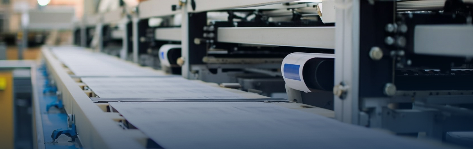
セラミック製品に加えて、当社は以下のような追加サービスも提供します。お客様のニーズに基づいて、お客様自身で製造したブランクまたは半完成ブランクを使用したカスタマイズされたセラミック加工サービス。外部委託のセラミックパッケージングおよびメタライゼーションサービスにご興味がございましたら、詳細についてお問い合わせください。当社は、お客様のさまざまなニーズを満たすワンストップ ソリューションを提供することに常に取り組んでいます。

はい、そうです。世界中のどこにお住まいであっても、ご注文の商品を安全かつタイムリーにお届けいたします。

お問い合わせを送信

アップロード
* File ONLY PDF/JPG./PNG. Available.
Submit Now

お問い合わせ

お問い合わせ
以下のフォームにできる限り記入してください。細かいことは気にしないでください。
提出する
Looking for ビデオ?
お問い合わせ #
19311583352

オフィスアワー

  • 月曜日から金曜日: 午前 9 時から午後 12 時、午後 2 時から午後 5 時 30 分

当社の営業時間は、グリニッジ標準時 (GMT) より 8 時間進んだ北京時間に基づいていることにご注意ください。お問い合わせや面談の日程調整につきましては、ご理解とご協力を賜りますようお願い申し上げます。お急ぎの場合や営業時間外のご質問につきましては、メールにてお気軽にお問い合わせください。できるだけ早くご連絡させていただきます。平素は格別のお引き立てを賜り、誠にありがとうございます。今後ともよろしくお願いいたします。

製品

whatsApp

接触