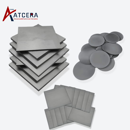
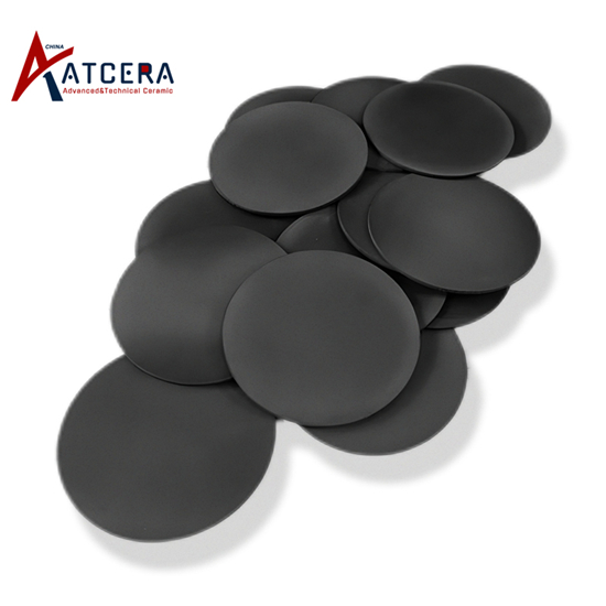
先端エレクトロニクスのダイナミックな世界では、常に先頭に立つための鍵は、絶え間ないイノベーションの追求にあります。テクノロジーが急速に進化し続ける中、高性能 Si3N4 半導体基板が業界に革命を起こす先駆者として台頭しています。優れた熱安定性、機械的強度、電気絶縁特性を備えた Si3N4 基板は、これまでにないほど先端エレクトロニクスの真の力を発揮します。
Si3N4 基板を電子機器に組み込むことで 、メーカーは性能と効率の限界を押し広げることができます。これらの基板は電子部品の電力処理能力を強化し、データ転送速度の高速化、熱管理の改善、信頼性の向上を実現します。スマートフォン、自動車用電子機器、航空宇宙用途など、Si3N4 基板はテクノロジーの体験方法を変えています。
高速で信頼性が高く、エネルギー効率に優れた電子機器の需要が高まり続ける中、Si3N4 半導体基板は業界を未来へと導く存在です。強度と絶縁特性のユニークな組み合わせにより、Si3N4 半導体基板は最先端の電子機器の開発に欠かせない要素となっています。
さあ、シートベルトを締めて、Si3N4 半導体基板がもたらす無限の可能性を探る準備をしましょう。先進的なエレクトロニクスの未来はここから始まります。
Si3N4半導体基板の利点
シリコン窒化物 (Si3N4) 半導体基板は、先進エレクトロニクスの世界でゲームチェンジャーとして登場し、業界に革命をもたらす数多くの利点を提供しています。Si3N4 基板の主な利点の 1 つは、その優れた熱安定性です。従来の半導体材料とは異なり、Si3N4 は構造的完全性や電気特性を損なうことなく高温に耐えることができます。この熱耐性は、パワーエレクトロニクス、高周波デバイス、自動車用電子機器など、電子部品が高熱にさらされるアプリケーションでは非常に重要です。
Si3N4 基板のもう 1 つの重要な利点は、その優れた機械的強度です。これらの基板は、高いレベルのストレスと歪みに耐える能力で知られており、耐久性と信頼性が最も重要となるアプリケーションに最適です。この機械的強度は、基板が敏感な電子部品から熱を効果的に逃がすことができるため、放熱性の向上にもつながり、システム全体のパフォーマンスと寿命が向上します。
さらに、Si3N4 半導体基板は優れた電気絶縁特性を備えており、これは高性能電子デバイスの設計と製造において重要な要素です。これらの基板は電気信号を効果的に分離し、クロストークを防ぎ、無線周波数 (RF) や高速デジタル回路などのアプリケーションに不可欠な信号の完全性を確保します。この絶縁特性は、Si3N4 ベースの電子デバイスの電力処理能力の向上にも貢献し、信頼性を損なうことなく、より高い電圧と電力レベルで動作できるようにします。
先端エレクトロニクスにおけるSi3N4半導体基板の応用
Si3N4 半導体基板の優れた特性により、幅広い高度な電子アプリケーションに欠かせないコンポーネントとなっています。パワーエレクトロニクスの分野では、Si3N4 基板は高出力トランジスタ、インバータ、モータードライブの製造に広く使用されています。これらの基板は必要な熱管理と電気絶縁を提供し、パワーエレクトロニクスデバイスがより高い電圧とスイッチング周波数で動作できるようにすることで、効率と信頼性が向上します。
自動車業界では、Si3N4 半導体基板が、特に電子制御ユニット (ECU) やその他の安全性が重要なコンポーネントの設計でますます普及しています。これらの基板の堅牢な機械的特性と熱安定性により、自動車用電子機器は、極端な温度、振動、衝撃など、車両内で発生する過酷な環境条件に耐えることができます。これにより、現代の自動車の全体的な信頼性と安全性が向上します。
航空宇宙および防衛分野でも、最高レベルのパフォーマンスと信頼性が求められることが多いため、Si3N4 半導体基板の使用が進んでいます。これらの業界では、レーダー、航空電子工学、衛星通信など、さまざまな電子システムで Si3N4 基板が使用されています。Si3N4 基板が提供する熱特性、機械特性、電気特性のユニークな組み合わせにより、航空宇宙および防衛分野での厳しい環境でも確実に動作できる高度な電子システムの開発が可能になります。
エレクトロニクス産業におけるSi3N4半導体基板の将来
より高速で、より効率的で、より信頼性の高い電子デバイスの需要が高まり続ける中、電子産業の将来を形作る上での Si3N4 半導体基板の役割は、いくら強調してもし過ぎることはありません。現代の電子システムの複雑さと電力要件がますます高まる中、Si3N4 基板の優れた特性により、製造業者や設計者にとって Si3N4 基板はますます魅力的な選択肢となっています。
Looking ahead, the integration of Si3N4 semiconductor substrates into a wide range of electronic devices is expected to accelerate. From next-generation smartphones and wearables to cutting-edge industrial automation and renewable energy systems, Si3N4 substrates will play a crucial role in enabling the development of high-performance, energy-efficient, and reliable electronic components.
Furthermore, the ongoing research and development in the field of Si3N4 substrate manufacturing processes are expected to drive further advancements in the technology. Improvements in material quality, manufacturing techniques, and cost-effectiveness will likely lead to the widespread adoption of Si3N4 substrates across the electronics industry, solidifying their position as the preferred choice for a wide range of applications.
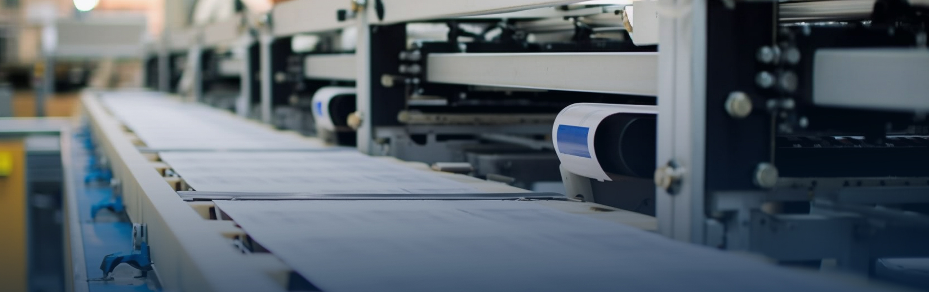
Manufacturing process of Si3N4 semiconductor substrates
The manufacturing of high-quality Si3N4 semiconductor substrates involves a complex and meticulous process that requires precise control over various parameters. The production of Si3N4 substrates typically begins with the synthesis of the raw material, silicon nitride, through a chemical reaction between silicon and nitrogen.
One of the most common methods for producing Si3N4 is the chemical vapor deposition (CVD) process, where silicon and nitrogen-containing precursor gases are introduced into a reaction chamber and subjected to high temperatures. This process allows for the controlled deposition of a thin, uniform layer of Si3N4 on a suitable substrate, such as silicon or sapphire.
Following the Si3N4 deposition, the substrate undergoes a series of precision machining and polishing steps to ensure a smooth, defect-free surface. This surface preparation is crucial, as it directly impacts the performance and reliability of the electronic devices that will be fabricated on the substrate.
To further enhance the properties of the Si3N4 substrate, various post-processing techniques may be employed, such as thermal annealing or the application of protective coatings. These additional steps help to optimize the substrate's thermal, mechanical, and electrical characteristics, making it better suited for specific electronic applications.
The manufacturing of Si3N4 semiconductor substrates requires a high level of expertise, advanced equipment, and stringent quality control measures to ensure the production of consistently reliable and high-performing materials. As the demand for these substrates continues to grow, manufacturers are continuously innovating and improving their processes to meet the ever-evolving needs of the electronics industry.
Key properties and characteristics of Si3N4 semiconductor substrates
The exceptional properties and characteristics of Si3N4 semiconductor substrates are what make them so valuable in the world of advanced electronics. One of the most notable features of Si3N4 is its exceptional thermal stability, which allows it to withstand high temperatures without compromising its structural integrity or electrical performance. This thermal resilience is particularly crucial in power electronics and high-power applications, where the substrate must be able to effectively dissipate heat generated by the electronic components.
In addition to its thermal stability, Si3N4 is renowned for its exceptional mechanical strength and hardness. These properties contribute to the substrate's ability to withstand high levels of stress and strain, making it an ideal choice for applications where durability and reliability are paramount, such as in automotive electronics and aerospace systems.
Another key characteristic of Si3N4 semiconductor substrates is their excellent electrical insulation properties. These substrates are highly effective at isolating electrical signals, preventing cross-talk and ensuring signal integrity, which is essential for high-frequency and high-speed digital circuits. This insulating capability also allows Si3N4-based electronic devices to operate at higher voltages and power levels without compromising reliability.
Furthermore, Si3N4 substrates exhibit a low coefficient of thermal expansion, which closely matches that of the semiconductor materials commonly used in electronic devices. This thermal compatibility helps to minimize the risk of thermal-induced stresses and failures, contributing to the overall reliability and performance of the electronic systems.
The combination of these exceptional properties – thermal stability, mechanical strength, electrical insulation, and thermal compatibility – makes Si3N4 semiconductor substrates a highly sought-after material in the electronics industry, enabling the development of cutting-edge electronic devices that are more powerful, efficient, and reliable than ever before.
Challenges and limitations of Si3N4 semiconductor substrates
While Si3N4 semiconductor substrates offer numerous advantages, they are not without their challenges and limitations. One of the primary challenges in the widespread adoption of Si3N4 substrates is the relatively higher cost compared to traditional semiconductor materials, such as silicon or gallium arsenide.
The manufacturing process of Si3N4 substrates is complex and requires specialized equipment, as well as a high level of expertise and quality control measures. This, in turn, can drive up the overall production costs, making Si3N4 substrates less accessible for some manufacturers, especially in price-sensitive markets.
Another limitation of Si3N4 substrates is their relatively lower thermal conductivity compared to some other semiconductor materials, such as silicon carbide (SiC) or diamond. While Si3N4 substrates exhibit excellent thermal stability, their ability to dissipate heat may be slightly less efficient in certain high-power applications, where the thermal management requirements are particularly demanding.
Additionally, the manufacturing of large-diameter Si3N4 substrates can be more challenging and may result in higher defect rates, limiting the availability of large-scale wafers for high-volume production. This can be a constraint for manufacturers who require larger substrate sizes to meet their specific design and production needs.
Despite these challenges, the electronics industry is continuously working to address the limitations of Si3N4 substrates through ongoing research and development.
Advancements in manufacturing processes, material engineering, and cost-reduction strategies are expected to help overcome these obstacles and further drive the adoption of Si3N4 substrates in the future.
Comparison of Si3N4 semiconductor substrates with other semiconductor materials
When it comes to semiconductor substrates, Si3N4 stands out as a unique and highly capable material, offering a combination of properties that are often unmatched by other semiconductor materials. One of the primary advantages of Si3N4 over traditional silicon (Si) substrates is its superior thermal stability and mechanical strength.
While silicon is a widely used semiconductor material, it can be susceptible to thermal degradation and mechanical failures at high temperatures or under high-stress conditions. In contrast, Si3N4 substrates can withstand much higher temperatures and exhibit greater resistance to mechanical stress, making them a better choice for power electronics, high-frequency, and harsh-environment applications.
Another semiconductor material that has gained significant attention in recent years is silicon carbide (SiC). Like Si3N4, SiC also offers excellent thermal stability and mechanical strength, making it a viable alternative for advanced electronic applications. However, Si3N4 substrates generally have a lower coefficient of thermal expansion, which can be advantageous in terms of thermal compatibility with semiconductor devices and reduced thermal-induced stresses.
Gallium nitride (GaN) is another semiconductor material that has seen increasing adoption in high-power and high-frequency electronics. While GaN-based devices can offer excellent performance, they often require specialized substrate materials, such as sapphire or SiC, to support their unique properties. In this context, Si3N4 substrates can serve as a cost-effective and compatible alternative, providing a suitable platform for the integration of GaN-based components.
In terms of electrical insulation properties, Si3N4 substrates outperform many other semiconductor materials, including silicon and gallium arsenide (GaAs). This superior insulation capability allows Si3N4-based electronic devices to operate at higher voltages and switching frequencies, improving overall efficiency and performance.
Overall, the unique combination of thermal, mechanical, and electrical characteristics of Si3N4 semiconductor substrates makes them a highly versatile and attractive choice for a wide range of advanced electronic applications, where the demand for high-performance, reliable, and efficient devices continues to grow.
Importance of high-performance Si3N4 semiconductor substrates in the development of advanced electronics
The role of high-performance Si3N4 semiconductor substrates in the development of advanced electronics cannot be overstated. As the electronics industry continues to push the boundaries of performance, efficiency, and reliability, these exceptional substrates have become an essential component in the quest for technological breakthroughs.
One of the key drivers behind the importance of Si3N4 substrates is the growing demand for power-dense and energy-efficient electronic devices. In industries such as automotive, aerospace, and renewable energy, the ability to handle high power levels while maintaining thermal stability and reliability is crucial. Si3N4 substrates, with their exceptional thermal management capabilities and mechanical strength, enable the design and manufacture of electronic components that can operate reliably under these demanding conditions.
Furthermore, the insulating properties of Si3N4 substrates are crucial in the development of high-frequency and high-speed electronic devices, such as those used in telecommunications, radar systems, and advanced computing. By effectively isolating electrical signals and preventing cross-talk, Si3N4 substrates help to ensure the integrity and performance of these mission-critical electronic systems.
As the world becomes increasingly reliant on advanced electronics, the need for reliable, durable, and efficient devices has never been more pressing. Si3N4 semiconductor substrates play a pivotal role in meeting these demands, enabling the creation of innovative electronic products that are better equipped to handle the challenges of the modern world.
From smartphones and wearables to industrial automation and renewable energy systems, the integration of high-performance Si3N4 substrates is transforming the electronics industry, paving the way for a future where advanced electronics are more powerful, efficient, and reliable than ever before.
Conclusion: The potential and outlook of Si3N4 semiconductor substrates in the electronics industry
エレクトロニクス業界が急速に進化を続ける中、先進エレクトロニクスの未来を形作る上で Si3N4 半導体基板の役割がますます明らかになっています。比類のない熱安定性、機械的強度、電気絶縁特性を備えたこれらの優れた材料は、これまで以上に強力で効率的、かつ信頼性の高い最先端の電子デバイスの開発において極めて重要な役割を果たすことになっています。
Si3N4 基板の可能性は大きく、パワーエレクトロニクスや高周波デバイスから自動車や航空宇宙システムまで、幅広い電子アプリケーションにシームレスに統合できます。高速で信頼性が高く、エネルギー効率の高い電子機器の需要が高まり続ける中、Si3N4 基板は技術革新の最前線に留まり、メーカーが可能性の限界を押し広げることを可能にします。
将来を見据えると、エレクトロニクス業界における Si3N4 半導体基板の将来は有望です。継続的な研究開発の取り組みにより、材料の品質、製造プロセス、コスト効率がさらに向上し、最終的には業界全体でこれらの基板が広く採用されることが期待されます。
エレクトロニクスの分野が進化し続ける中、Si3N4 基板の汎用性と性能は、最先端の高性能電子デバイスの追求においてますます欠かせないコンポーネントとなるでしょう。ポケットの中の洗練されたスマートフォンから航空機の高度な航空電子工学システムまで、Si3N4 基板の影響は幅広い業界に及んでおり、私たちが知っているテクノロジーの未来を形作っています。
結論として、電子産業における Si3N4 半導体基板の可能性は、まさに無限です。より高速で、より効率的で、より信頼性の高い電子デバイスの需要が高まり続ける中、これらの優れた材料は、間違いなく、高度な電子工学の新時代を先導し、私たちが周囲の世界と関わり、体験する方法を変革する上で極めて重要な役割を果たします。